The Designer's Guide Community
Forum
Welcome, Guest. Please Login or Register. Please follow the Forum guidelines.
Apr 25th, 2024, 3:38pm
Pages: 1
Send Topic Print
About connection of the Filter and VCO in PLL design (Read 7216 times)
gaom9
Junior Member
**
Offline


Posts: 21
CHINA
About connection of the Filter and VCO in PLL design
Mar 06th, 2009, 5:50pm
 
Hi,
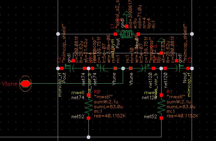
I am working in a Δ-Σ Fractional-N Frequency Synthesizers, I have a question about the connection of the filter and VCO in the circuit. The varactor of the VCO is AMOS as shown in Fig.1, the Vtune Voltage is directly connected to one port of the AMOS.


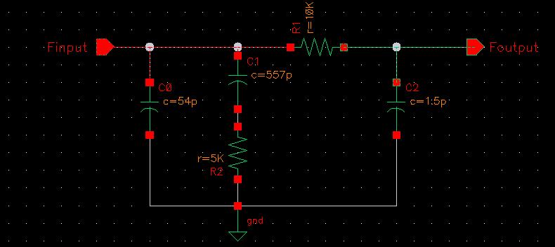
The loop filter is off-chip and 3order as shown in Fig.2.


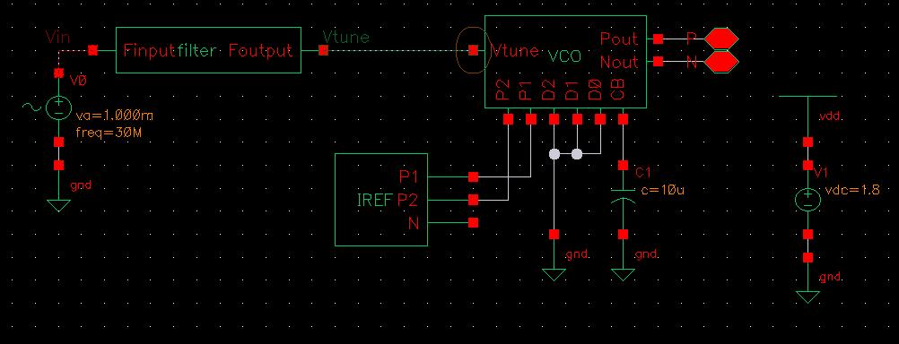
In the total circuit system connection, I connect the Filter and VCO directly, but, I found, the Vtune Voltage after the loop filter will be distorted, and a large current flow in to/out from the VCO, and this makes a large spurious tones to the Voltage signal, and makes it not stable. The voltage added to the filter (Vin), voltage after the filter (Vtune) and the current into the VCO are shown in Fig. 3
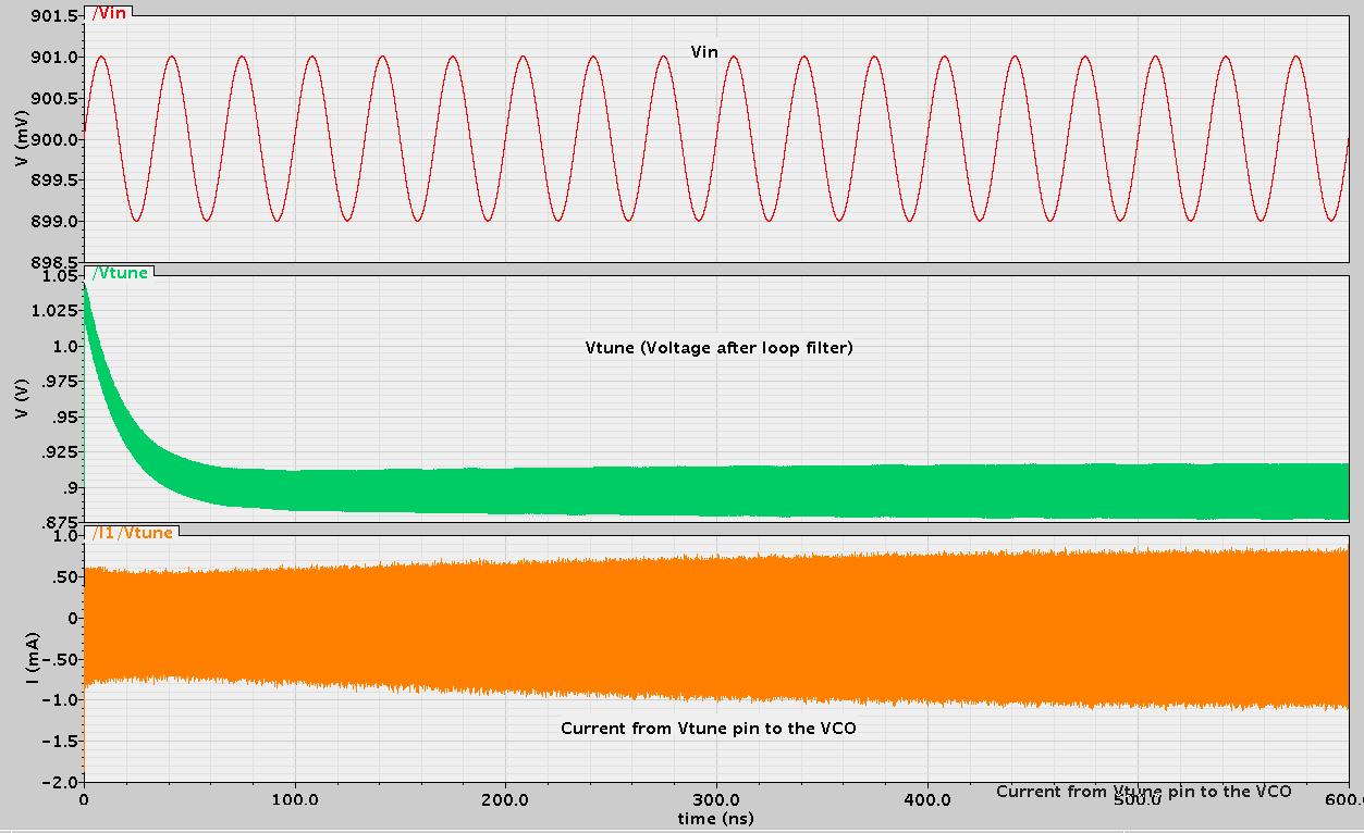


And I think I only need the Voltage value in VCO tune, the Current is unwanted, and I should removal the current, is that right?
I try to add a large resistor between the filter and the VCO to limit the current, and the VCO work well, but what I worry is that is the method right? what value the resistor shoule be and shoule it be off-chip? and is the resistor added here will effect the loop filter zero/pole? Or should I make any change in the VCO tune voltege input pin design, please?

Thank you!
Best regards!

Back to top
 
 
View Profile gaom9   IP Logged
gaom9
Junior Member
**
Offline


Posts: 21
CHINA
Re: About connection of the Filter and VCO in PLL design
Reply #1 - Mar 7th, 2009, 6:56am
 
The varactor is biasing to 1/3*Vdd. The DC biasing voltage is added from the 40K resistor in the two side of the varactor, should it right? Or should I change the biasing point.
In this AMOS, when biasing it to 1/3*Vdd the capacitor will be more linear in the whole range 0~1.8V.
Back to top
 
 
View Profile gaom9   IP Logged
gaom9
Junior Member
**
Offline


Posts: 21
CHINA
Re: About connection of the Filter and VCO in PLL design
Reply #2 - Mar 9th, 2009, 12:04am
 
Hi
I am sorry I made a mistake, when I add a large resistor between the filter and the VCO input, the current unwanted can be limited, but the VCO tune Voltage is still have a large dither. Adding a large resistor can not solve this question.
And I add a large capacitor to ground at the connect line between filter and VCO, the AC current will be filter out, but the bandwidth will be change...
So, is there any mistake in my filter design? But I find this type of filter is used in many papers.
Back to top
 
 
View Profile gaom9   IP Logged
gaom9
Junior Member
**
Offline


Posts: 21
CHINA
Re: About connection of the Filter and VCO in PLL design
Reply #3 - Mar 10th, 2009, 3:26am
 
I know the filter is driven by the charge pump current. But my question is that when I use the 3rd order filter, the voltage in the two edge of R1 is not the same, and the voltage of the charge pump output is with much less dither than the voltage at the tune voltage node of the VCO.
Yestoday, I try to used the 2nd order filter, and because there is not resistor between the output node of charge pump and the input node of VCO, the voltage can keep the same. But when the tune voltage keep stable, the VCO output is with large dither, either. I think the input current of the VCO result in this dither, this current go through the DC biasing resistor and change the DC bias point of the varactor.  
How to reduce this effect?

When I used the PSS simulation to analyse the VCO alone, the VCO can work well with a certian DC tune input.

And how to make sure the Voltage added between the varactor keep stable when the Vtune voltage is stable so the keep the capactor of varactor the same and a DC biasing is added to one node of the varactor, please?

I tried to used three 3MΩ resistors to generator Vdd/3 dc biasing voltage, and for the so large resistors, the DC bias can keep stable, and the output is with less dither, but the resistors are too large....
How can I generator a Vdd/3 DC voltage, please?

Thank you!
Best regards
Back to top
 
« Last Edit: Mar 10th, 2009, 4:35am by gaom9 »  
View Profile gaom9   IP Logged
gaom9
Junior Member
**
Offline


Posts: 21
CHINA
Re: About connection of the Filter and VCO in PLL design
Reply #4 - Mar 13th, 2009, 5:54am
 
Back to top
 
 
View Profile gaom9   IP Logged
rfmems
Senior Member
****
Offline


Posts: 121

Re: About connection of the Filter and VCO in PLL design
Reply #5 - Apr 16th, 2009, 8:07am
 
Hi gaom9,

Sorry but I have to say what you are simulating is completely wrong. When you drive your loop filter with a voltage signal, the voltage sees only a rc fliter for 3rd order and a short for 2nd ord.

The tuning voltage gets bigger than your input might because your vco is unbalanced not becuase the loop filter itself.

I think you are not going anywhere with the settings you have.

Looking at the loop filter alone, C2 is too small you have to  check carefully the load of the VCO.
Back to top
 
 
View Profile   IP Logged
macrohan
New Member
*
Offline


Posts: 7

Re: About connection of the Filter and VCO in PLL design
Reply #6 - Aug 14th, 2009, 2:14am
 
you should using a current source replace voltage source to drive your loop filter.
Back to top
 
 
View Profile macrohan   IP Logged
loose-electron
Senior Fellow
******
Offline

Best Design Tool =
Capable Designers

Posts: 1638
San Diego California
Re: About connection of the Filter and VCO in PLL design
Reply #7 - Aug 22nd, 2009, 3:04pm
 
one important item - do not put the filter outside the chip

you are going to pick up a lot of noise going in/out of the chip and your phase noise (jitter) is going to suffer a lot.

Wont be seen in simulation. Will be suffered with in silicon.

Been there, done that.
Back to top


Jerry Twomey
www.effectiveelectrons.com
Read My Electronic Design Column Here
Contract IC-PCB-System Design - Analog, Mixed Signal, RF & Medical
View Profile WWW   IP Logged
Pages: 1
Send Topic Print
Copyright 2002-2024 Designer’s Guide Consulting, Inc. Designer’s Guide® is a registered trademark of Designer’s Guide Consulting, Inc. All rights reserved. Send comments or questions to editor@designers-guide.org. Consider submitting a paper or model.